GRiDCASE 1537E hardware
Last revised: 19 Jan 2001
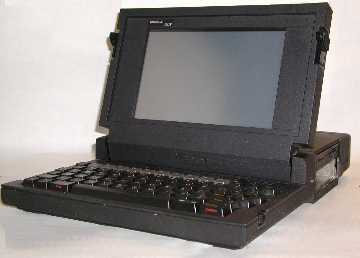
Front view
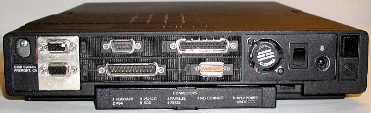
Rear view
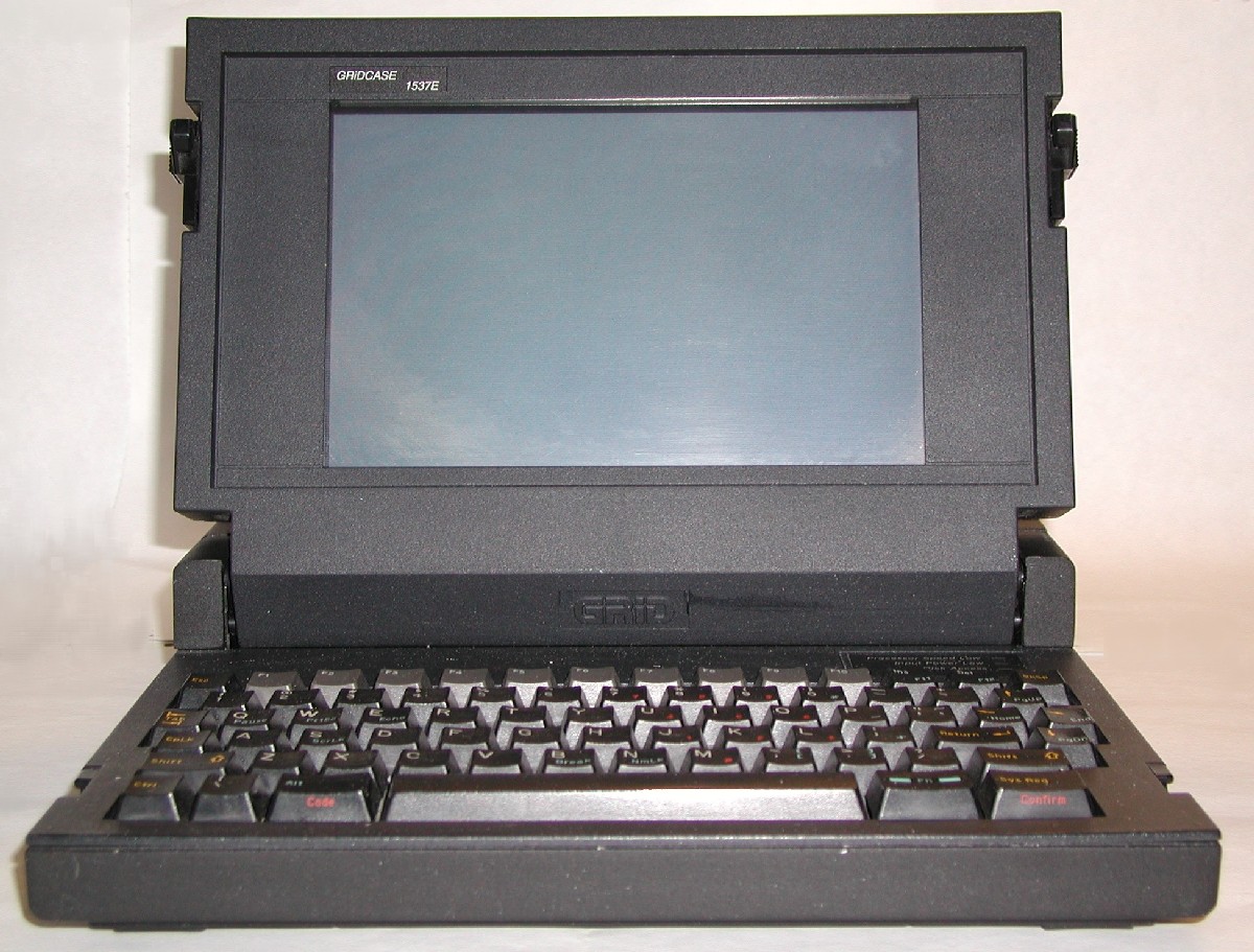
Front view
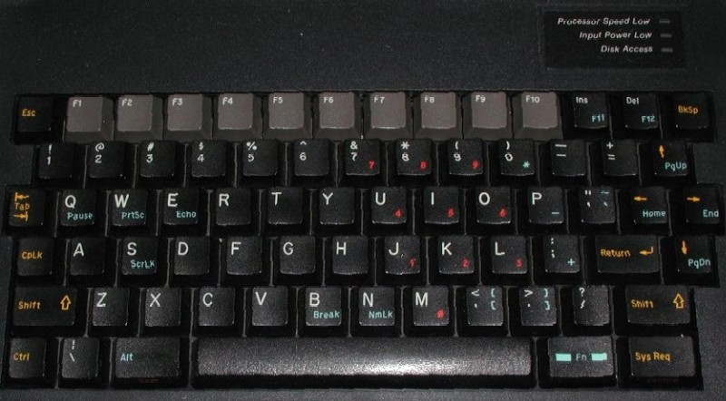
Keyboard
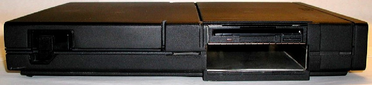
Right view
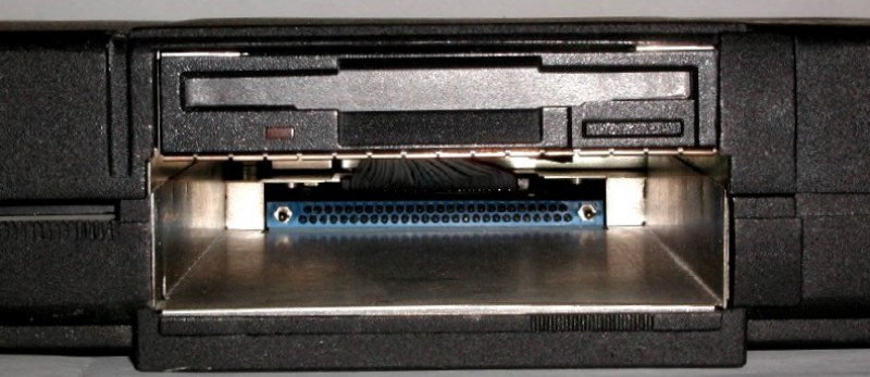
HDD slot
|
GRiDCASE 1537E hardware Last revised: 19 Jan 2001 |
|
|
Front view |
Rear view |
Front view |
Keyboard |
Right view |
HDD slot |
Table1, Onboard chips
| Chip | Type |
|---|---|
| U1 | 14069U (Motorola) |
| U2 | 74HC125A |
| U3 | 74HC125D |
| U4 | 74AC04 |
| U5 | 74HC04 |
| U6 | P5C060-45 |
| U7 | 74HC125A |
| U8 | P8742AH KB CONTRLR 5/19/88 (D8F1) 300782-04 AK |
| U9 | 74HC137N |
| U10 | 74HC157N |
| U11 | DS3692N |
| U12 | AM26LS32ACN |
| U13 | LM339 |
| U14 | F82C636 |
| U15 | 74AC74 |
| U16 | AC04 |
| U17 | HC257N |
| U18 | HC257N |
| U19 | MC3488AP1 |
| U20 | HC74D |
| U21 | AC08 |
| U22 | AC08 |
| U23 | DS1000M |
| U24 | P5C032-35 |
| U25 | I387 |
| U26 | P5C032-35 |
| U27 | AM85C30-16JC |
| U28 | TL16C452FN |
| U29 | HC125D |
| U30 | F82C206 |
| U31 | F82C841 |
| U32 | |
| U33 | AC08 |
| U34 | I80386-16 |
| U35 | P5C060-45 |
| U36 | 74HCT244A |
| U37 | AM26LS32ACN |
| U38 | AC573 |
| U39 | 74AC244 |
| U40 | 74AC244 |
| U41 | 74AC245 |
| U42 | P5C032-35 |
| U43 | F82C842 |
| U44 | AIC-6260AL |
| U45 | 74AC244 |
| U46 | MAX241CW1 |
| U47 | 74AC244 |
| U48 | 74AC244 |
| U49 | 74AC245 |
| U50 | 74AC245 |
| U51 | 74AC244 |
| U52 | SIMM 30 pin |
| U53 | SIMM 30 pin |
| U54 | SIMM 30 pin |
| U55 | SIMM 30 pin |
| U56 | SIMM 30 pin |
| U57 | SIMM 30 pin |
| U58 | SIMM 30 pin |
| U59 | SIMM 30 pin |
| U60 | HCT245A |
| U61 | HCT245A |
| U62 | OKI M41464-12 |
| U63 | OKI M41464-12 |
| U64 | 74AC244 |
| U65 | AM27C512 |
| U66 | AM27C512 |
| U67 | OKI M41464-12 |
| U68 | OKI M41464-12 |
| U69 | Bt476KPJ35 |
| U70 | OKI M41464-12 |
| U71 | OKI M41464-12 |
| U72 | F82C455 |
| U73 | 74AC244 |
| U74 | LM339M |
| U75 | OKI M41464-12 |
| U76 | OKI M41464-12 |
| U77 | 74HC157N |
The design is based on LeAPset CS8283 CHIPSet, that comprises highly integrated application specific integrated circuits that emulate the control logic of IBM PC AT-compatible computers. Additionally, this chipset provides functions designed specifically for the laptop comp.
BIOS features and hot keys:
· (Ctrl,Alt - Tab) Toggle built in/external display
· (Ctrl,Alt - BkSp) toggles built in mode (positive/negative image)
· To boot from floppy, you can hold down the "F" key during boot and it should boot from the floppy unless it is dead
· To force boot from HDD, you can hold down the "H" key during boot
BIOS checksums:
· 52A2 for EVEN
· 185E for ODD
| Internal HDD connector |
Connector model:
| HYPERTRONICS CAGE/FSCM50541 KA53/127BPMB10T-554 9101 |
As I was unable to find any suitable female part of this connector on the market, Ive bought two 40-pin SIP sockets, cutted them to appropriate length and glued them together an got nice 53-pin socket. Power connector was replaced by standard coax as well. Power supply unit works fine with my Compaq portable mains power supply ( 19V, 3A).
Table 2
| Pin # | Direction | IDE socket pin | Description | Signal path [pin #] chip |
|---|---|---|---|---|
|
53
|
---> | Power connector | +12 V Power | Q4 |
|
52
|
---> | Power connector | +12 V Power | Q4 |
|
51
|
---> | Power connector | +12 V Power | Q4 |
|
50
|
---> | Power connector | +12 V Power | Q4 |
|
49
|
---> | Power connector | +12 V Power | Q4 |
|
48
|
---> | Power connector | +5 V Power | Q2 |
|
47
|
---> | Power connector | +5 V Power | Q2 |
|
46
|
---> | Power connector | +5 V Power | Q2 |
|
45
|
---> | Power connector | +5 V Power | Q2 |
|
44
|
---> | Power connector | +5 V Power | Q2 |
|
43
|
---- | Power connector | Power ground | |
|
42
|
<==> | 18 | Data 15 | [18] U61 <=> [2] U61 <=> [102] U43 |
|
41
|
---- | Signal ground | ||
|
40
|
<==> | 16 | Data 14 | [17] U61 <=> [3] U61 <=> [101] U43 |
|
39
|
---- | Signal ground | ||
|
38
|
---- | Signal ground | ||
|
37
|
<==> | 17 | Data 0 | [11] U60 <=> [9] U60 <=> [84] U43 |
|
36
|
<==> | 14 | Data 13 | [16] U61 <=> [4] U61 <=> [100] U43 |
|
35
|
<==> | 15 | Data 1 | [12] U60 <=> [8] U60 <=> [85] U43 |
|
34
|
<==> | 12 | Data 12 | [15] U61 <=> [5] U61 <=> [99] U43 |
|
33
|
---- | Signal ground | ||
|
32
|
---- | Signal ground | ||
|
31
|
<==> | 13 | Data 2 | [13] U60 <=> [7] U60 <=> [86] U43 |
|
30
|
<==> | 10 | Data 11 | [14] U61 <=> [6] U61 <=> [98] U43 |
|
29
|
<==> | 11 | Data 3 | [14] U60 <=> [6] U60 <=> [87] U43 |
|
28
|
<==> | 8 | Data 10 | [13] U61 <=> [7] U61 <=> [97] U43 |
|
27
|
---- | Signal ground | ||
|
26
|
---- | Signal ground | ||
|
25
|
<==> | 9 | Data 4 | [15] U60 <=> [5] U60 <=> [88] U43 |
|
24
|
<==> | 6 | Data 9 | [12] U61 <=> [8] U61 <=> [96] U43 |
|
23
|
<==> | 7 | Data 5 | [16] U60 <=> [4] U60 <=> [92] U43 |
|
22
|
<==> | 4 | Data 8 | [11] U61 <=> [9] U61 <=> [95] U43 |
|
21
|
---- | Signal ground | ||
|
20
|
---> | 23 | /IOW | [14] U36 <- [6] U36 |
|
19
|
<==> | 5 | Data 6 | [17] U60 <=> [3] U60 <=> [93] U43 |
|
18
|
---> | 25 | /IOR | [1] U33,[6] U35 <- [35] U31 |
|
17
|
<==> | 3 | Data 7 | [18] U60 <=> [2] U60 <=> [94] U43 |
|
16
|
---- | Signal ground | ||
|
15
|
---- | Signal ground | ||
|
14
|
<--- | 31 | IRQR | -> [8] U36 -> [12] U36 -> [80] U30 |
|
13
|
---> | ??? 28 ALE | <- [9] U36 <- [11] U36 | |
|
12
|
---- | Signal ground | ||
|
11
|
<--- | HDD latched | -> [3] U22 -> [4] U22 -> [37] U14 (PIO11) | |
|
10
|
---> | 33 | DA1 | |
|
9
|
<--- | ??? 27 IO_CH_RDY | -> [2] U36 <- [18] U36 | |
|
8
|
---- | Signal ground | ||
|
7
|
---- | Signal ground | ||
|
6
|
---> | 35 | DA0 | <- [7] U36 |
|
5
|
---> | 36 | DA2 | <- [3] U36 |
|
4
|
---> | ??? 37 /IDE_CS0 | <- [17] U35 <- | |
|
3
|
---> | ??? 38 /IDE_CS0 | <- [18] U35 <- | |
|
2
|
<--- | 39 | /ACTIVE Led | -> [1] U5 -> |
|
1
|
---- | 2 | Signal ground |
| SHARP LJ64AU31 gas plasma display (VGA 640x480) |
SHARP guys appeared being not much user-friendly lol, so I failed to get any info from them. No any old datasheets on their pages - no any traces of these gas plasma modules on SHARP sites.
Table 3, Gas plasma display unit connector pinout
| Display socket pin # | Function | Wire color | Ext Plug pin |
|---|---|---|---|
|
1
|
Ground (Serial Data 1) | Dark Blue | 1 |
|
2
|
Serial Data 1 | Red | 2 |
|
3
|
Ground (Serial Data 2) | Green | 3 |
|
4
|
Serial Data 2 | Yellow | 4 |
|
5
|
Ground (Serial Clock) | White | 5 |
|
6
|
Serial Clock | Brown | 6 |
|
7
|
Ground (V Frame Sync) | Grey | 7 |
|
8
|
V Frame Sync | Black | 8 |
|
9
|
Ground (H Frame Sync) | Orange | 9 |
|
10
|
H Frame Sync | Blue | 10 |
|
11
|
NC | ||
|
12
|
Ground | Dark Blue | 11 |
|
13
|
Ground | ||
|
14
|
Power (+5V) | Black/White | 12 |
|
15
|
Power (+5V) | Red/White | 13 |
|
16
|
Ground | ||
|
17
|
Ground | ||
|
18
|
Power +24 V | ||
|
19
|
Power +24 V | Yellow/White | 14 |
|
20
|
Power +24 V | Blue/White | 15 |
All data and clock inputs (2,4,6,8,10) are loaded internally with 60-Ohm resistors. All data wires are twisted in pairs.
PCB has 6 x Hitachi ECN2012 on the left side and 6 x Hitachi ECN2002 chips mounted on the right side on flex PCB.
8xSHARP LZ1440 and 8 more items are mounted on top and bottom sides of the PCB.
These flex PCBs are connected to the main PCB by four 15-wire flat flex cables.
In the center of the board SHARP LZ93N34 and Toshiba TC54256AF (EPROM) chips are mounted. There are also two SHARP PC9D17 chips soldered.